The 7 Stages Of Designing A Custom PCB Panel


PCB (printed circuit board) panel design can be a complex process and there are many considerations that have to be made when establishing a project timescale. In this article, we explain the seven main stages of a custom PCB design service, to give you an idea of what’s involved (in some cases there are up to 18 stages involved, including finishing and testing). These are, of course, very general approximations. If you’d like to discuss a PCB design or prototype with one of our team in person, and receive a more accurate and personalised estimate, please give us a call today.
A PCB schematic is like a blueprint that shows engineers what components are used on the board, how they fit together, and how they interact. Simple PCB panels can be designed using a flat schematic, which is like a 2-D map of the board when viewed from above. However, as the interactions between groups of components can be complicated, some designs require a hierarchical schematic, which blocks groups of components together in terms of function and relationship, making the design easier to conceptualise and edit. From the schematic, you can use PCB design software to define the size, shape, dimensions and layers for your circuit board.
Your PCB schematic then needs to be configured with your specific application data, including a full breakdown of the components and nets required. This can be compiled manually or automatically, depending on the design program used.
The layer stack comprises the footprint of your printed board. Most modern circuit boards have four layers, although some have many more. At the design stage, it’s important to consider the materials you will be using, and your printing methods. At the stack up stage you can choose from a range of laminates and materials to protect your board and enhance performance. For example, with high-frequency or high-speed PCBs, impedance control can be built into the physical arrangement of the stack.
Each category of PCB has a wide range of rules and standards – not all of which are relevant to your design. At this stage of the design process, you choose the appropriate rules and constraints to guide the manufacturing process. These should reflect your device specifications and the PC board’s operational tolerances. Some design programs allow you to select or deselect these rules, but if you are designing manually you’ll need to consult your component data sheets to select the appropriate design rules.
Custom PCB panel design gives you great flexibility over where to place your components. Consideration should be given to component workflows and how these interact together as a circuit. A professional design service will ensure that each component is placed according to layout best practices, and in the most efficient component groups. Key design considerations are where to place your drill holes, as this will affect the routing of your traces. Following on from this, anchor parts should be positioned first, followed by the main circuitry and bypass caps, before other related circuitry and resistors are positioned.
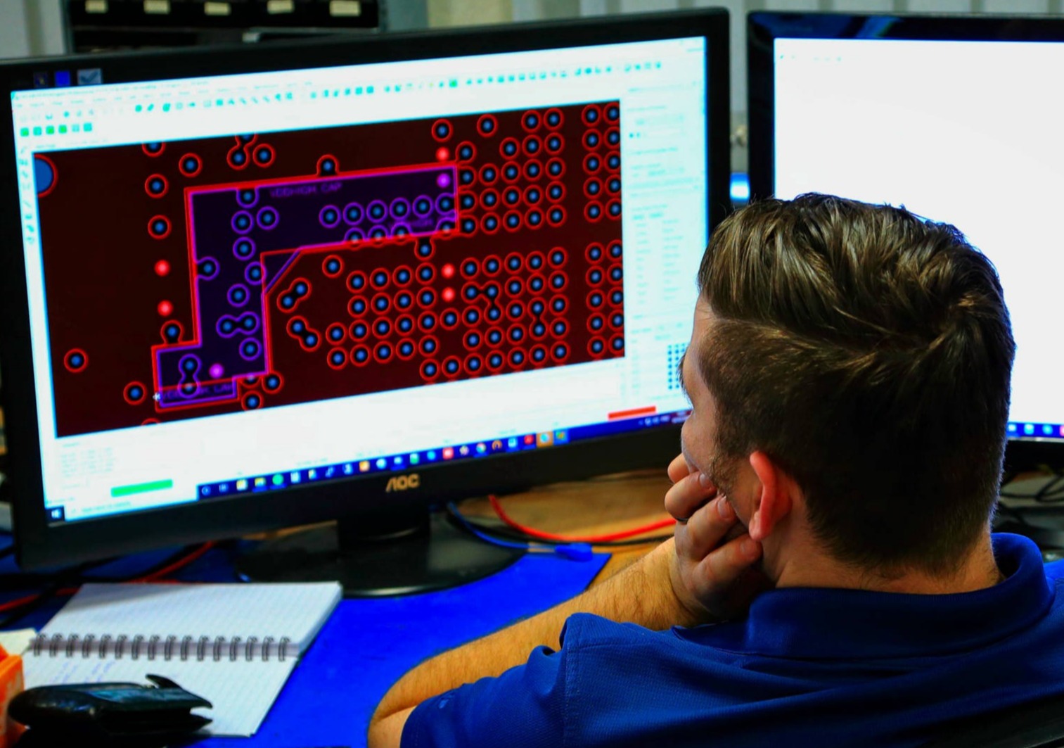
Route tracing is a testing process that creates virtual pathways between components, to verify the position and design of the PCB. Colour-coded route tracing lets you track a range of routes and determine the most efficient design layout for your PCB.
With the layout in place and verified, it is now time to add whatever markings, labels, and position identifiers required for PCB engineers to make sense of the design, and to facilitate accurate manufacturing. You can then create design files for your PCB that contain all the data required to print your board. The standard format for PCB files – widely used since 1980 – is RS274-D (with X1 or X2 variants), commonly known as the Gerber format. However, a variety of alternative CAD file formats are now available, so consult with your PCB manufacturing partner to confirm which files are compatible with their CNC equipment.
At HGL Systems we specialise in custom PCB panel design for product prototype and low-volume runs, with a wide range of CAD and CNC equipment that lets us handle the entire end-to-end process in-house. To find out more, or to request a free quote, please get in touch today.
Follow Us